Chris Ward's 6502 Computer
![]()
| News |
| Introduction |
| Specifications |
| The Circuit |
| Parts List |
| Programming |
| EEPROM Programmer |
| Photographs |
| Downloads |
| Related Links |
Back to my Home Page |
Created by Chris Ward
Last update 15/05/2007
(DD/MM/YYYY)
Here are the schematics, produced with xfig for Linux. You can download the original xfig files as well as PNG or GIF versions:
- Part 1 - 6502 and support circuitry: xfig PNG GIF
- Part 2 - Address Decoding and Memory: xfig PNG GIF
- Part 3 - I/O Devices: xfig PNG GIF
- Keypad Interface: xfig PNG GIF
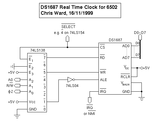
- DS1687 Real Time Clock: xfig PNG GIF
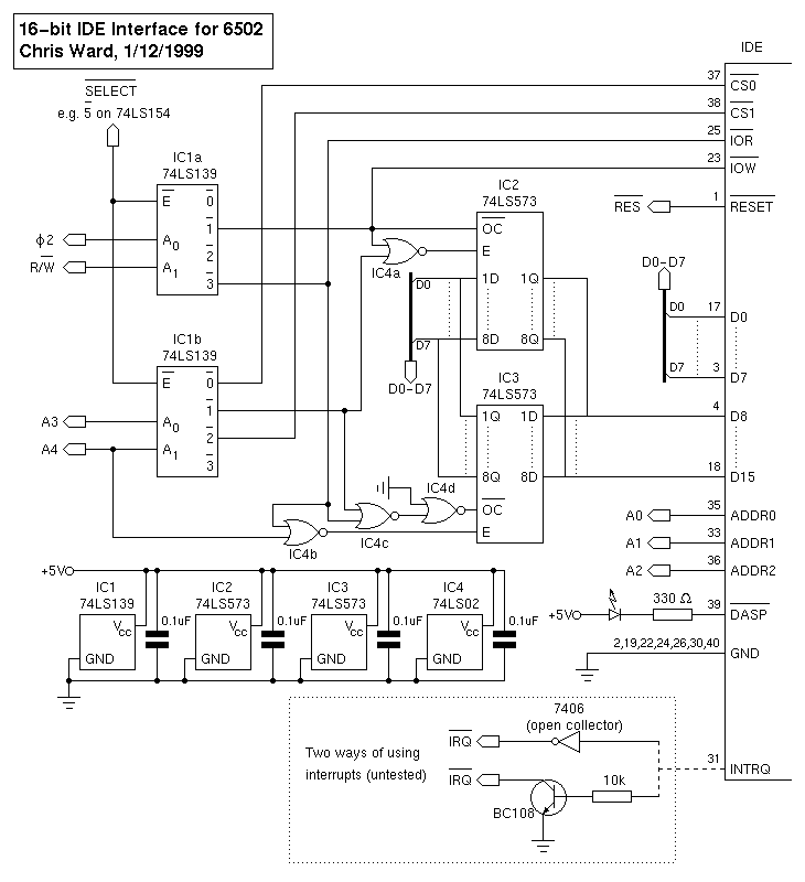
- IDE Interface: xfig PNG GIF
Click here to download a ZIP file containing my stripboard layouts in Traxmaker 3 format.
[ There's an old version of this page here which might give you an insight into how the circuit has developed. It's not really worth it though :-) ]
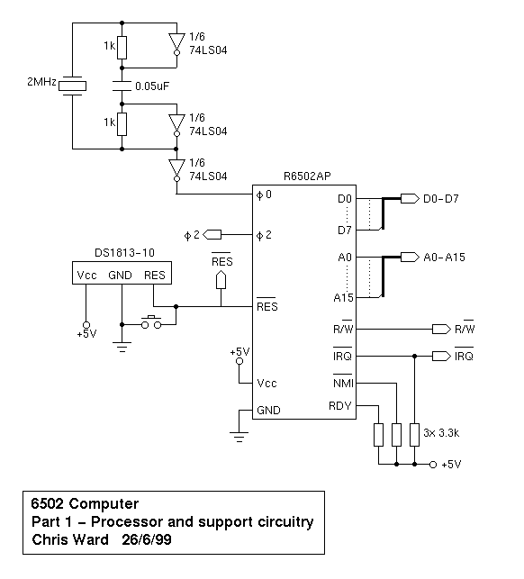
Clock, Reset and other bits around the CPU
Credit to Harry The Bastard for the clock circuit. A 2MHz crystal is used, plus three inverters from a 74LS04, two 1k resistors and one 0.05uF capacitor. Harry's page will tell you more about how it works - but suffice it to say that it does work.
The reset circuit is basically just a single IC - the Dallas DS1813-10. This 3-pin device will pull the reset line low when the power supply is out of range (e.g. during power-up) and also gives a reset pulse when you press a pushbutton connected between RES and GND.
Also around the CPU are some 3k3 pull-up resistors on the IRQ, NMI and RDY pins. Does anyone know if S.O. (Set Overflow) should also be tied high?
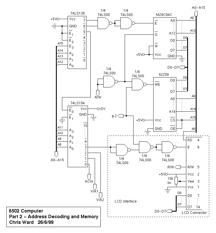
Address Decoding
The A15 line is connected straight to the chip select and output enable pins of the 32k SRAM chip. Hence, if A15 is low (access to bottom 32k of memory) then the RAM is selected. Logic gates are used to activate the RAM's write enable when R/W is low (i.e. write) and the phase 2 clock is high. This assumes that write enable always overrides output enable (check your RAM's data sheet if you want to be sure).
If A15 is high, then the 74LS138 (3-to-8 decoder) is enabled and looks at A12-A14. The eight outputs correspond to 4k blocks of memory in the range $8000-$FFFF.
Outputs 6 and 7 of the '138 ($E000-$FFFF) are combined by an AND gate (made with two NANDS from a 74LS00) to provide the chip select for the EEPROM. This needs some thinking about due to the active-low inputs and outputs, but draw the truth table and it all makes sense. Output enable is provided by inverting the R/W line, and write enable is tied high because we will never write to this device.
Output 5 of the '138 selects the 4k of I/O space at $D000-$DFFF. This activates the 74LS154 (4-to-16 decoder) which looks at A8-A11 to divide the I/O space into sixteen 256-byte segments. Each of the sixteen outputs will act as chip select for a particular I/O device.
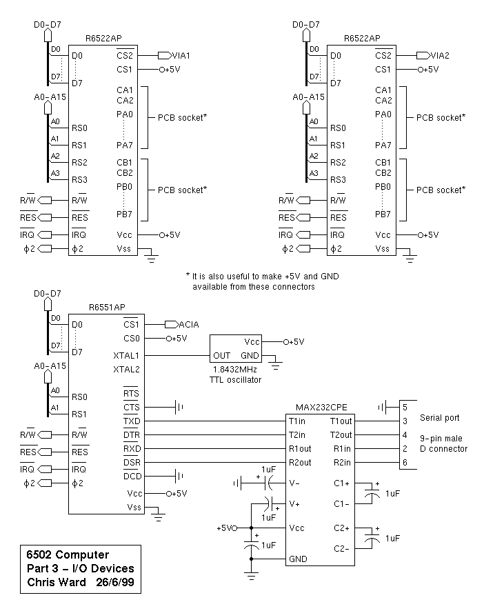
The VIAs and ACIA
There are two 6522 VIAs. Their chip selects are connected to outputs 1 and 2 of the 74LS154, which maps them to $D100 and $D200. They have the usual connections to the address, data and control busses, and all their I/O lines are made available on PCB connectors.
The 6551 ACIA is connected up in a similar way to the VIAs, and is mapped to $D000. A 1.8432MHz TTL oscillator module is connected to XTAL1 - this is is used by the 6551 to produce the various baud rates. Two RS232 output lines (TXD, DTR) and two RS232 input lines (RXD, DSR) are made available to the outside world via a MAX232CPE. This device converts 0V/5V logic level signals to RS232 levels (about +10V/-10V I think). A few capacitors are needed between certain pins as shown on the data sheet. (Note: you could use the MAX233, which doesn't need these external capacitors)
LCD Interface
An interface is provided for industry-standrad alphanumeric displays, which have 14 pins and a Hitachi HD44780 controller (my LCD uses the Epson SED1278, which is compatible with the HD44780).
The LCD is interfaced directly to the 6502's bus. The data lines D0-D7 and the R/W line are connected straight across, and address line A0 connects to RS (register select). The Enable signal is derived from output 3 of the 74LS154, which maps the LCD to $D300. This is gated by the phase 2 clock pulse to synchronise the LCD with the bus.
A contrast control is provided by a 10k linear potentiometer between +5V and GND with the wiper contact connected to Vee on the LCD.
Other Little Bits
Well, there's the power indicator. I use a nice bright blue LED (is this the first computer with a blue power LED?) with a 150 ohm series resistor. This value was scientifically determined (sort of) from the quoted forward voltage in the catalogue, and some equation which escapes me right now.
I've also placed 0.1uF decoupling capacitors (some ceramic, some polysester, I don't think it matters) between +5V and GND as close as possible to all the major ICs.
I haven't shown the infra-red receiver on the schematics, but it's very simple. I use a Kodenshi PIC26043SM, which has three legs: one goes to +5V, one goes to ground, and one goes to a spare I/O pin on one of the 6522s.